For AI and Cloud Servers, High-Precision and High-Reliability DDR5 Memory Power Solutions
Kunhung Chen, Payne Lin, Frank Chang, Sophia Tong | AN093
With the rapid development of cloud computing, big data, and AI applications, server memory power topologies are
facing increasing challenges, including high precision, low noise, high reliability, and high energy efficiency.
Richtek introduces a series of highly integrated power management IC solutions for DDR5 server memory. By
leveraging fast compensation control loops, intelligent voltage regulation, and comprehensive protection
mechanisms, our solutions ensure stable memory operation while enhancing overall system reliability and
efficiency. This product family not only improves power efficiency and system robustness but also helps customers
address diverse application requirements and accelerates the evolution of next-generation server platforms.
1. Key Challenges in Server Memory Power Design
With the continued growth of cloud computing data analytics and AI workloads modern servers are required to
support ever higher memory capacity and bandwidth. As memory density and speed increase, power delivery
requirements become significantly more stringent. Server memory power design must therefore address a set of
critical challenges, including voltage accuracy, reliability, efficiency, and thermal management.
1.1 Ultra-High Voltage Accuracy and Low Noise Under Low Voltage Tolerance
High voltage accuracy is essential to ensure stable memory operation. DDR5 memory exhibits extremely tight voltage
tolerance, and even minor voltage deviations can lead to data corruption or system instability. Therefore, power
supplies must deliver exceptional regulation accuracy and ultra-low output noise.
Table 1. Output Voltage Specific
|
VDD |
VDDQ |
VPP |
| Typical Output Voltage |
1.1V |
1.1V |
1.8V |
| DC + AC Tolerance |
+/-2.5% |
+/-2.5% |
+/-2.5% |
| DC Accuracy |
+/-0.75% |
+/-0.75% |
+/-0.75% |
Note 1. Refer to JESD301-5 and PMIC5030 Specification for additional information.
1.2 Long-Term Reliability Under Hot-Plug and Transient Overvoltage Conditions
High reliability is a fundamental requirement in server power supply design. Servers are expected to operate
continuously over extended periods and any power related failure may lead to data loss or service interruption
resulting in substantial economic impact. As a result, power management ICs must incorporate comprehensive
protection features including overvoltage, overcurrent, and over-temperature protection while system components
must provide adequate overvoltage tolerance to support long term stable operation.
In server memory power applications, hot plug conditions are a critical reliability concern. Memory modules typically
require both a high voltage 12V rail and a low voltage 3.3V rail. Due to the layout of the module golden fingers a
temporary short circuit between these two supplies may occur during insertion or removal, as illustrated in Figure 1.
This scenario places significant stress on the power management ICs, which must tolerate such fault conditions
without damage. Sufficient overvoltage robustness is therefore essential to ensure system integrity and prevent
module failure.
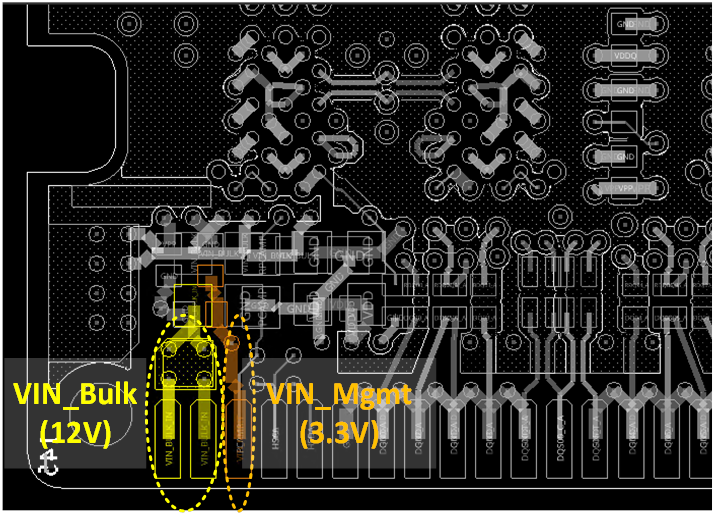
Figure 1. RDIMM Golden Finger Diagram (VIN_BULK and VIN_MGMT are Adjacent Pins)
1.3 Efficiency and Thermal Stability in High Power Density Architectures
Energy efficiency and thermal management represent additional critical challenges in server power design. Server
environments consume substantial amounts of energy and improvements in power conversion efficiency directly
reduce operating costs while contributing to lower overall carbon emissions. Furthermore, as power density
continues to increase effective thermal management and the prevention of overheating become essential design
considerations.
In the DDR5 generation, the power management IC is mounted directly on the memory module, rather than on the
motherboard as in previous DDR4 designs, as illustrated in Figure 2. This architectural change significantly
increases the local power density on the memory module, which in turn places greater emphasis on efficiency
optimization and accurate temperature monitoring to ensure reliable operation.
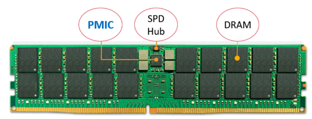
Figure 2. DDR5 RDIMM Memory Module
2. Richtek DDR5 Memory Power Solutions
To address the design challenges of reliability, voltage accuracy, efficiency, and thermal management discussed
above, Richtek has developed a comprehensive range of server memory power solutions. Through careful circuit
architecture design, component selection, system-level integration, and application-level validation, these solutions
are designed to enhance overall performance and long-term reliability.
For each DDR5 server memory specification including different capacity and data rate configurations, Richtek
provides optimized and application-specific power solutions to support a wide range of system requirements as
summarized in Table 2 and Table 3. Detailed product specifications are available on the Richtek website or through
our sales representatives.
Table 2. Richtek Server DDR5 PMIC Solution Series
| Generation |
Server Low Current |
Server High Current |
Server Extreme Current |
Sever Extreme Current Gen2 |
| JEDEC Standard |
P5010 |
P5000 |
P5020 |
P5030 |
| Richtek Solution |
RTQ5119A |
RTQ5150A |
RTQ5152 |
RTQ5153 |
| Application |
RDIMM |
RDIMM, CXL MM |
RDIMM, MRDIMM, CXL MM |
RDIMM, MRDIMM, CXL MM |
| Generation |
Server Low Current |
Server High Current |
Server Extreme Current |
Sever Extreme Current Gen2 |
Table 3. DDR5 PMIC Applications for Different DIMM Capacities and Transfer Rates
| Card |
Config. |
DRAM
Density |
DIMM
Capacity |
DDR5 Transfer Rate (MT/s) |
| 4400 |
4800 |
5600 |
6400 |
7200 |
8000 |
>=8800 |
| RDIMM |
1Rx8 |
16 Gb |
16 GB |
RTQ5119A
(P5010) |
RTQ5119A or RTQ5150A
(P5010/5000) |
RTQ5152
(P5020) |
RTQ5153
(P5030) |
| 24 Gb |
24 GB |
| 32 Gb |
32 GB |
| 2Rx8 |
16 Gb |
32 GB |
| 24 Gb |
48 GB |
RTQ5150A
(P5000) |
RTQ5150A or RTQ5152
(P5000/5020) |
| 32 Gb |
64 GB |
4Rx8
(DDP) |
16 Gb |
64 GB |
| 24 Gb |
96 GB |
| 32 Gb |
128 GB |
| 2Rx4 |
16 Gb |
64 GB |
| 24 Gb |
96 GB |
| 32 Gb |
128 GB |
4Rx4
(3DS, SDP or DDP) |
16 Gb |
128 GB |
RTQ5152
(P5020) |
| 24 Gb |
192 GB |
| 32 Gb |
256 GB |
8Rx4
(3DS) |
16 Gb |
256 GB |
| 24 Gb |
384 GB |
| 32 Gb |
512 GB |
| MRDIMM |
2Rx8 |
16 Gb |
32 GB |
RTQ5152
(P5020)
MR - 8.8GT/s |
|
RTQ5153
(P5030)
MR - 12.8GT/s and above |
|
| 24 Gb |
48 GB |
| 32 Gb |
64 GB |
| 4Rx8 |
16 Gb |
64 GB |
| 24 Gb |
96 GB |
| 32 Gb |
128 GB |
| 2Rx4 |
16 Gb |
64 GB |
| 24 Gb |
96 GB |
| 32 Gb |
128 GB |
4Rx4
(3DS, SDP or DDP) |
16 Gb |
128 GB |
| 24 Gb |
192 GB |
| 32 Gb |
256 GB |
3. Advantages of Richtek DDR5 Memory Power Solutions
3.1 High-Precision, Low-Noise Power Control Architecture
First, in terms of high-precision voltage regulation, Richtek adopts an advanced A2RCOT voltage feedback control
topology, combined with a high-precision reference voltage source and low-noise design, ensuring output voltage
error is less than ±0.75%. In addition, built-in compensation and automatic calibration mechanisms effectively
minimize the effects of temperature drift and load variation on the output voltage, meeting the stringent power
accuracy requirements of memory modules. The following sections explain temperature characteristics, load
regulation, and dynamic response in detail. Further information on the A2RCOT voltage feedback control topology
can be found in the relevant product datasheet.
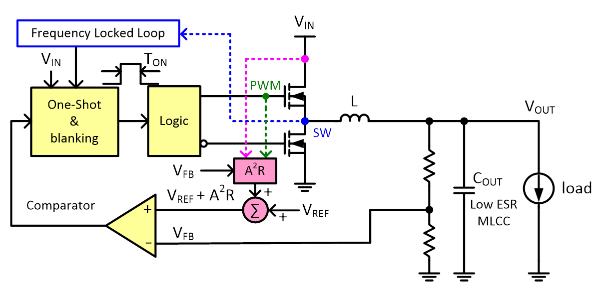
Figure 3. A2RCOT Control Loop
3.1.1 Excellent Temperature Compensation Characteristics Compliant with JEDEC Standards
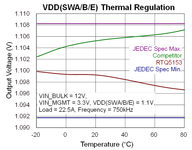
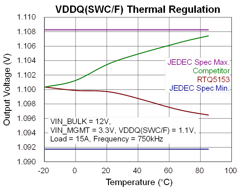
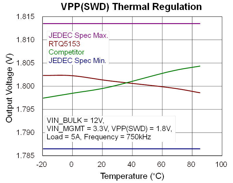
Figure 4 to Figure 6 compare the output voltage characteristics of the RTQ5153 with a major competing device across
different temperature conditions. In server DDR5 applications, temperature stability of the power management IC is
critical, as servers are typically required to operate continuously over extended periods under harsh thermal
environments, including both high and low temperatures. Any deviation in output voltage may compromise memory
data integrity and overall system stability.
Across the temperature range from ?20°C to 80°C, the RTQ5153 maintains a highly stable output voltage profile,
with voltage variation well below the JEDEC specification limit of ±0.75%. Compared with competing solution, the
RTQ5153 exhibits smaller output voltage deviation at both temperature extremes, demonstrating superior
temperature stability.
|
|
|
|
Figure
4. VDD(SWA/B/E) Output Voltage and Temperature Variation
|
Figure 5. VDDQ(SWC/F) Output Voltage and Temperature Variation
|
|
|
|
|
Figure
6. VPP(SWD) Output Voltage and Temperature Variation
|
|
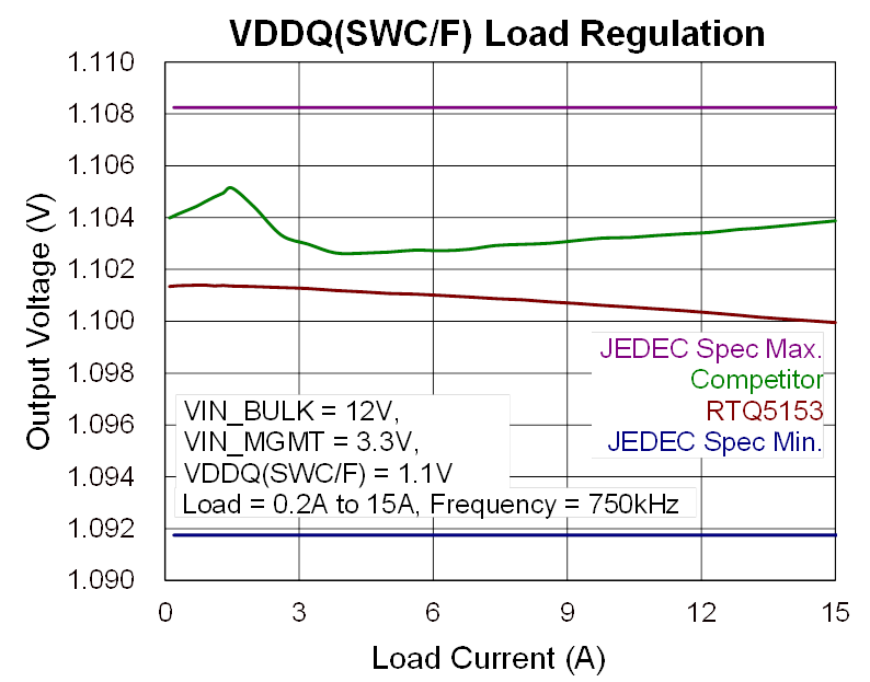
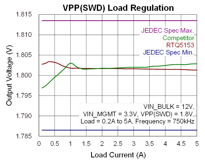
3.1.2 Precise Output Voltage Regulation Compliant with JEDEC
Standards
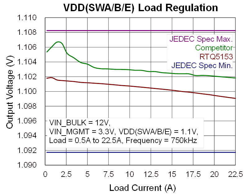
Figure 7 to Figure 9 compare the output voltage characteristics of the RTQ5153 with a major competing device under
different load conditions. In server DDR5 memory applications, the power management IC must be capable of
responding to dynamic memory load variations while continuously delivering stable and accurate output voltage.
Excessive voltage deviation can result in data transmission errors system instability and degraded overall server
performance.
Under a wide range of load transient, the RTQ5153 maintains a smooth and stable output voltage profile with
voltage variation well below the JEDEC specification limit of ±0.75%. Compared with the competing solution, the
RTQ5153 exhibits superior load regulation performance.
|
|
|
|
Figure
7. VDD(SWA/B/E) Output Voltage and Load Variation
|
Figure 8. VDDQ(SWC/F) Output Voltage and Load Variation
|
|
|
|
|
Figure
9. VPP(SWD) Output Voltage and Load Variation
|
|
3.1.3 Fast and Real-Time Dynamic Response
Richtek’s DDR5 power management IC series incorporates advanced power control topology to deliver high output
stability. An integrated fast compensation loop enables rapid detection of load transients and immediate control
response significantly reducing output voltage droop during sudden load changes and ensuring stable and reliable
system operation.
In addition, an intelligent output voltage overshoot suppression mechanism is implemented. During load release
conditions, the control loop responds promptly by actively disabling the low side switch thereby effectively limiting
excessive output voltage excursion and preventing potential component stress or abnormal system behavior caused
by voltage overshoot. Table 4 presents a load step comparison between Richtek solutions and a competing device
demonstrating superior performance across a range of test conditions.
Table 4. Load Step Comparison between Richtek and Competitors
3.2 High Reliability and Multiple Protection Mechanisms
For high reliability design, Richtek’s solution features multiple protection mechanisms, including overvoltage,
overcurrent, short-circuit, and over-temperature protection, as shown in Figure 10, ensuring immediate response
and system safety in abnormal conditions. In addition, for server applications, Richtek provides higher input pin
voltage tolerance, addressing potential short-circuit and overvoltage issues that may occur during memory module
insertion and removal, further enhancing system availability and fault tolerance.
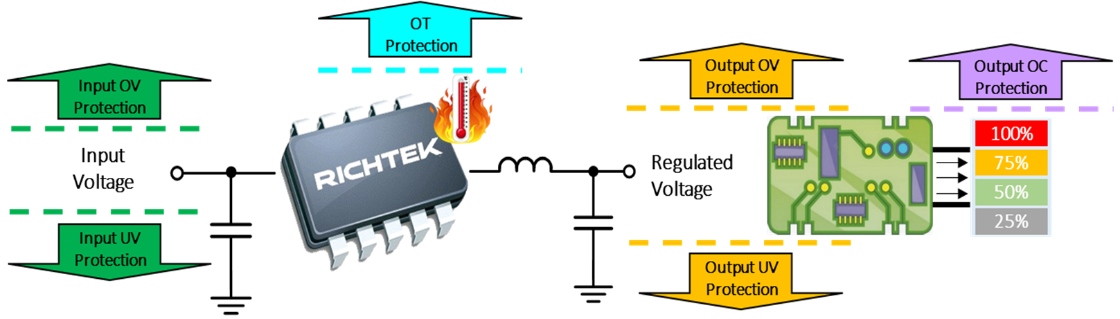
Figure
10. DDR5 PMIC Protection Features
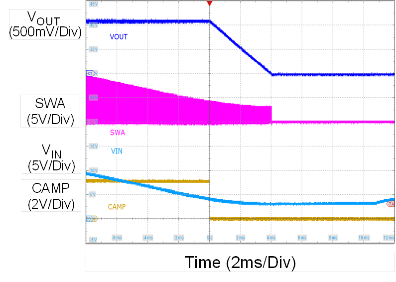
3.2.1 Input Overvoltage and Undervoltage Protection Mechanisms
Input overvoltage and undervoltage protection are essential to prevent component overstress and abnormal operation
during power fault conditions, such as surge events, hot plug spike, low input voltage, or power source mismatch, as
shown in Figure 11 and Figure 12. Input overvoltage can lead to capacitor or MOSFET breakdown while undervoltage
conditions may result in brownout, data read/write errors, and repeated system resets.
When an abnormal input condition is detected, the protection mechanism immediately disables the downstream VR and
sets a corresponding fault flag in the register. This allows the system to transition rapidly into a safe
operating state perform fault diagnosis and recover normal operation once the condition is cleared. Such
protection improves long term system reliability and component lifetime, while reducing maintenance and warranty
costs mitigating potential safety risks and maintaining overall operational stability.
Richtek products provide various threshold setting options for input overvoltage and undervoltage protection,
enabling system designers to implement comprehensive and application specific protection schemes. Detailed
information is available in the relevant product datasheets.
|
|
|
|
Figure
11. Input Overvoltage Protection
|
Figure
12. Input Undervoltage Protection
|
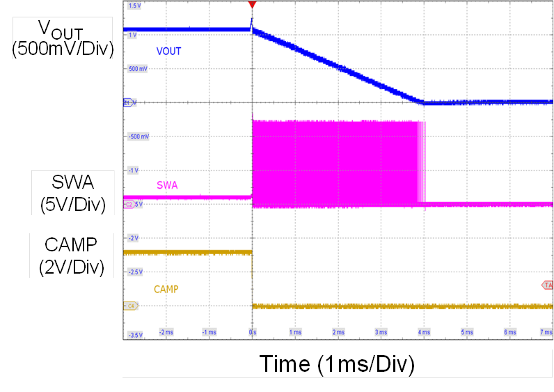
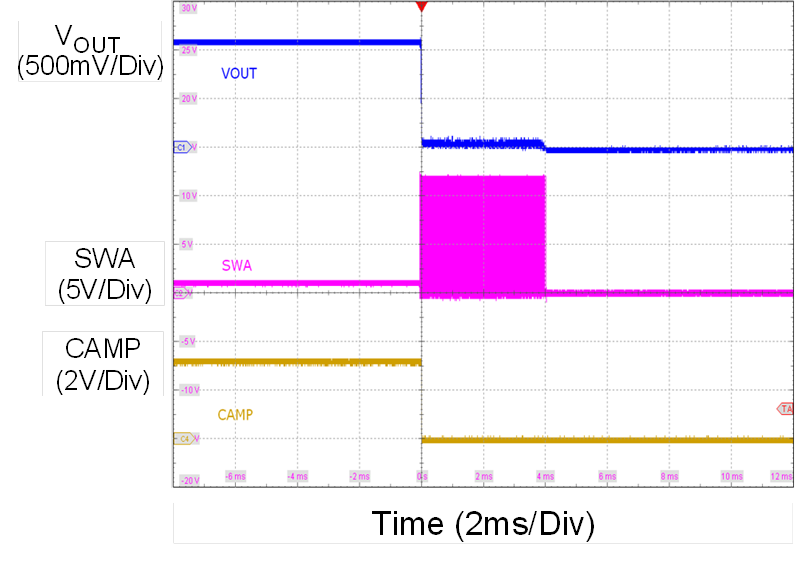
3.2.2 Output Overvoltage and Undervoltage Protection Mechanisms
Output overvoltage and undervoltage protection are required in the system to ensure that downstream DRAM is not
damaged by abnormal voltages and to maintain overall stable operation, as shown in Figure 13 and Figure 14. Output
overvoltage may cause component breakdown and overheating, while output undervoltage can lead to data
read/write errors and repeated system restarts. When the output voltage exceeds the allowable range, the system
immediately shuts down and withdraws the Power-Good signal to report a fault, allowing the system to quickly enter
a safe state, prevent fault propagation, and facilitate diagnosis and recovery. This also improves reliability and meets
DRAM voltage range specifications. Richtek products offer various threshold settings for output overvoltage and
undervoltage protection, making it convenient for system designers to plan comprehensive system protection.
Detailed information is available in the relevant product datasheets.
|
|
|
|
Figure
13. Output Overvoltage Protection
|
Figure
14. Output Undervoltage Protection
|
3.2.3 Output Overcurrent Protection Mechanism
Output overcurrent protection is necessary because situations, such as output short circuits, overloads, or inrush currents during parallel loading can cause the output current to exceed the design limit. This may lead to overheating and damage of the IC, inductor, and PCB traces, as well as voltage drops, instability, or even safety risks. As shown in Figure 15, the overcurrent protection mechanism limits the current when an abnormal condition occurs. If necessary, it immediately shuts down the output and withdraws the Power-Good signal to report a fault, quickly cutting off energy to prevent fault propagation. Working together with over-temperature and undervoltage protection, it enables controlled recovery, improves reliability and lifespan, meets safety and quality requirements, and reduces maintenance costs. Richtek products offer various threshold settings for output overcurrent protection, allowing system designers to plan appropriate overcurrent protection according to actual system loads. Detailed information is available in the relevant product datasheets.
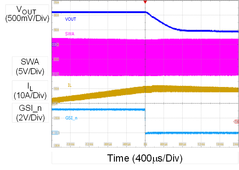
Figure
15. Output Overcurrent Protection
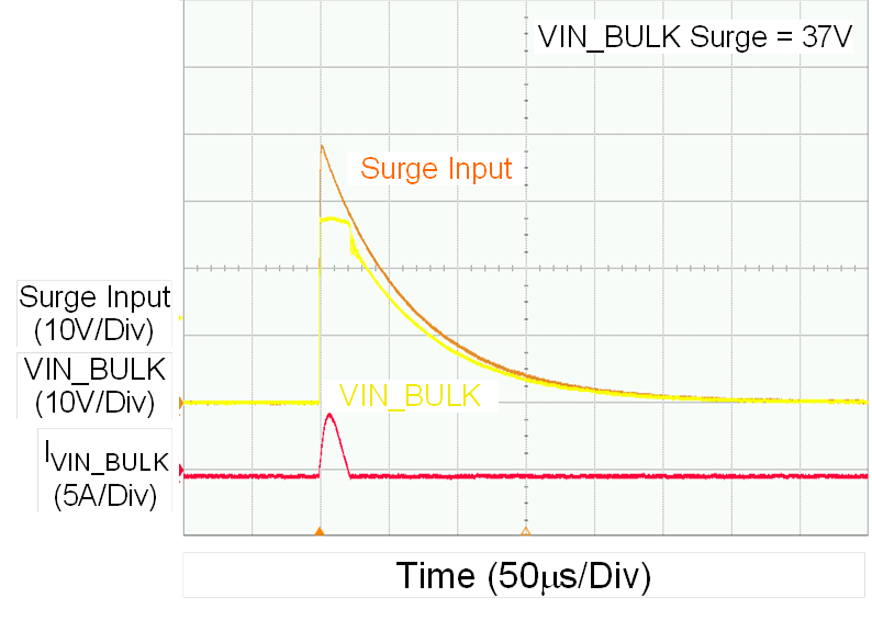
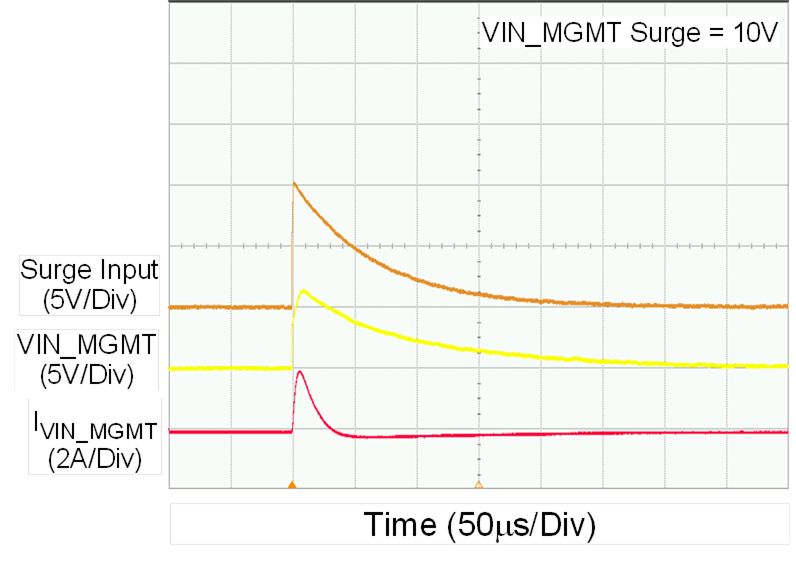
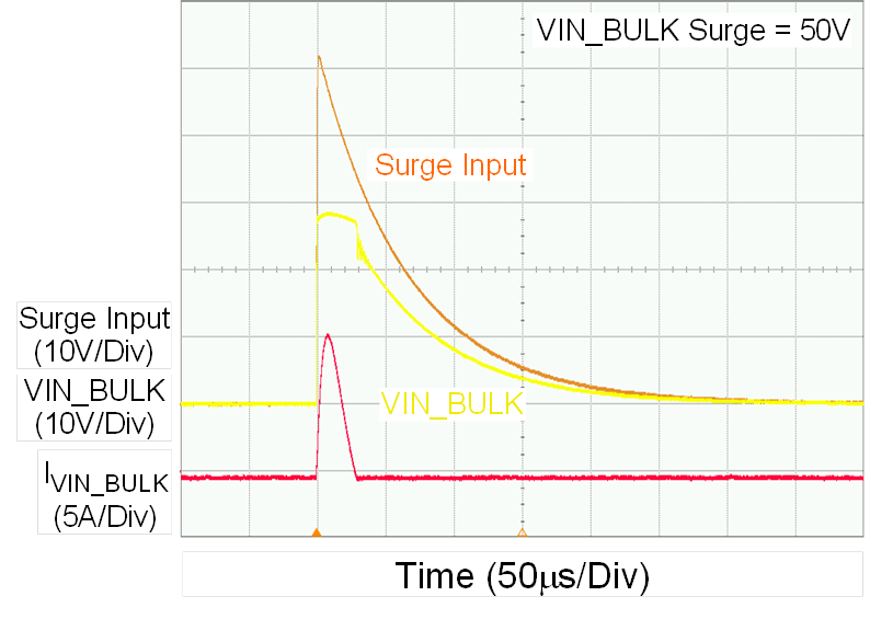
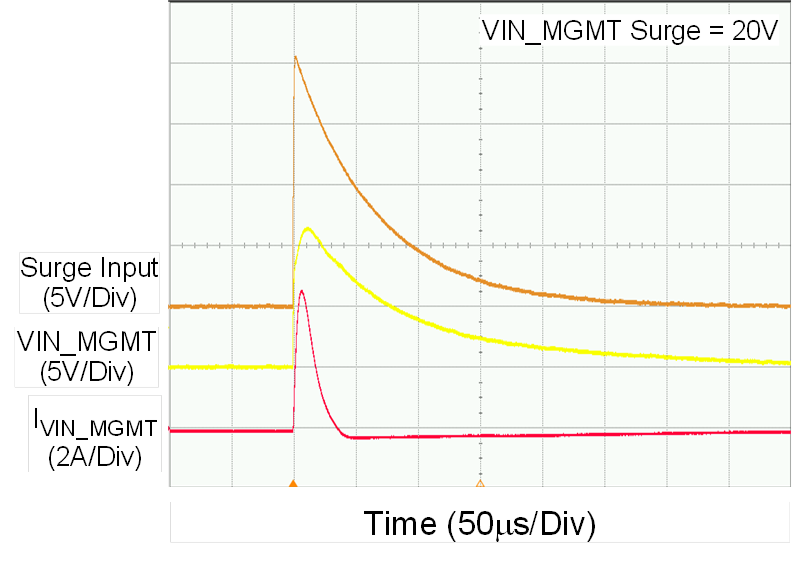
3.2.4 JEDEC-Compliant EOS Component Withstand Voltage Test
EOS (Electrical Overstress) protection capability is a key indicator for ensuring product reliability. For the two input
terminals of the DDR5 server power solution series, pulse voltage tests of 37V and 10V were conducted in
accordance with JEDEC standards to simulate possible transient high-voltage scenarios, as shown in Table 5.
After rigorous testing, Richtek products not only fully meet the standard requirements but also demonstrate higher
tolerance. This enhanced robustness allows the devices to withstand electrical overstress events encountered in
real world operating conditions while maintaining stable operation thereby providing improved safety margin and
long-term reliability for system designers.
Table
5. Vin_Bulk and Vin_Mgmt Input Pin EOS Test Results
|
VIN_BULK Pin EOS Test Results
|
VIN_MGMT Pin EOS Test Results
|
|
|
|
|
|
|
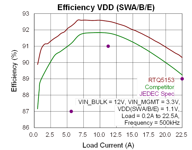
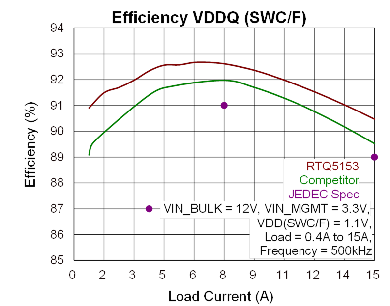
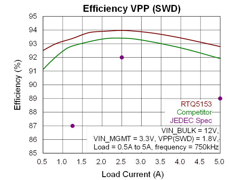
3.3 High Efficiency and Enhanced Thermal Management
In server DDR5 memory applications, the efficiency of the power management IC has a direct impact on overall
system energy consumption, thermal design margin, and operating cost. To address efficiency and thermal
management requirements, Richtek implements high-efficiency synchronous rectification, achieving power
conversion efficiency above 92%, thereby reducing both power loss and heat dissipation.
In addition, accurate ADC-based temperature monitoring, together with over-temperature protection, ensures stable
operation under high load conditions and prevents junction temperature from exceeding component limits. This
approach extends component lifetime and enhances long-term server system reliability.
Through optimized circuit design and advanced semiconductor manufacturing processes, Richtek products further
improve conversion efficiency. As demonstrated by the test results in Figure 16 to Figure 18, Richtek products not
only exceed JEDEC specification requirements but also outperform the average efficiency level of comparable
competing solutions. Under identical operating conditions, this higher efficiency translates into lower overall server
power consumption, reduced thermal stress, and eased thermal management design constraints, resulting in lower
system energy cost.
|
|
|
|
Figure
16. VDD(SWA/B/E) Efficiency
|
Figure 17. VDDQ(SWC/F) Efficiency
|
|
|
|
|
Figure
18. VPP(SWD) Efficiency
|
|
3.3.1 High Temperature Warning Reporting Mechanism
Richtek products for DDR5 server applications feature high-precision temperature reporting, automatically activating protection mechanisms when the temperature reaches 85°C to ensure safe system operation. The temperature reporting error at each stage is controlled within ±5°C, as shown in Table 6, providing accurate and reliable temperature monitoring. This feature not only meets stringent regulatory requirements but also greatly enhances product safety and stability in various application environments.
Table 6.
Temperature Measurement
| PMIC Ambient Temperature |
PMIC Temperature Measurement |
| 85°C |
85°C |
| 95°C |
96°C |
| 105°C |
106°C |
| 115°C |
117°C |
| 125°C |
127°C |
| 135°C |
138°C |
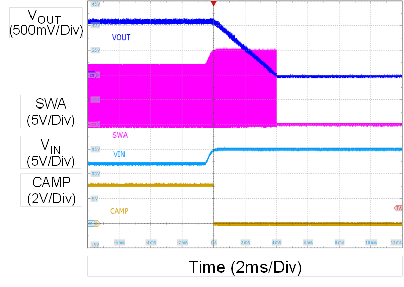
3.3.2 Over-Temperature Protection Mechanism
Richtek products feature a built-in over-temperature protection mechanism. When the temperature exceeds 145°C, the system immediately activates protective measures, shutting down all output voltages, as shown in Figure 19, and accurately reports the fault status through the Power-Good signal. This design effectively prevents damage caused by overheating, ensures safe operation of the equipment, and allows users to promptly monitor the system’s health status, thereby enhancing overall reliability.
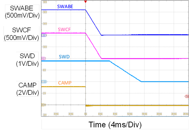
Figure
19. Over-Temperature Protection
Conclusion
Richtek’s server memory power solutions satisfy the requirements of high-end server platforms across key performance metrics, including voltage accuracy, dynamic response, reliability and efficiency. By employing high-precision feedback and a fast compensation topology, stable output is maintained across load and temperature variations, providing sufficient power margin for DDR5 memory during high-speed operation and reducing the risk of system instability.
Multiple protection and status reporting mechanisms are integrated to enhance platform fault tolerance and support long-term reliable operation. In parallel, high-efficiency, low-loss power design reduces power consumption and heat dissipation, easing thermal design requirements and improving overall system energy efficiency.
All solutions comply with Intel power specifications and AVL requirements, and have been validated at system level by multiple DRAM manufacturers. This enables direct integration into mainstream server platforms while shortening development and validation timelines.
By combining core power management expertise with extensive server platform experience, Richtek continues to optimize power architecture and circuit design to deliver competitive memory power solutions. Ongoing R&D investment, together with close collaboration across the ecosystem, further drives improvements in server platform performance and reliability.
To stay informed with more information about our products, please subscribe to our newsletter.